- The chain has five links: design, wafer fabrication, assembly and test, packaging, and distribution — with an equipment and materials layer supplying all of them.
- Singapore is unusual in hosting every link at once. It produces roughly a tenth of the world's chips and about a fifth of global semiconductor equipment output.
- Singapore's strength is mature and specialty process nodes, packaging and test, and equipment — not leading-edge logic. That is a deliberate position, not a shortfall.
- A design is developed against one foundry's process design kit and is not portable. Second-sourcing generally means redesign, a new mask set and full requalification.
- The 2026 build-out is the largest in the country's history: Micron broke ground on a US$24 billion fab in January, and UMC's 22nm fab reaches volume production this year.
What the semiconductor value chain actually is
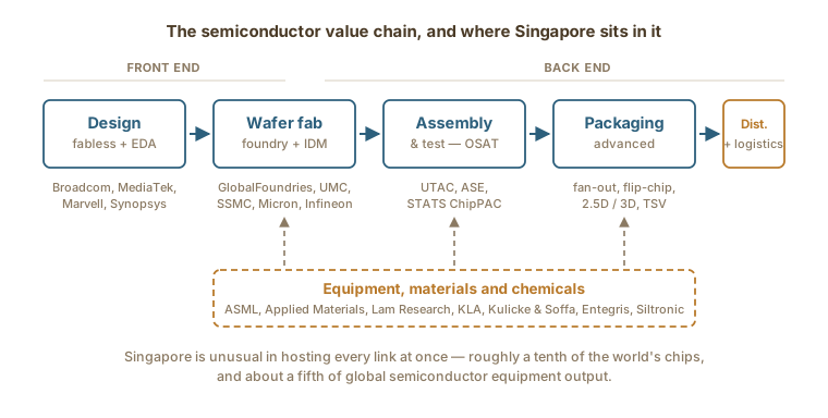
Design: fabless, IDM and EDA
- Fabless companies design but do not manufacture. They own the circuit design and the customer relationship, and they buy manufacturing capacity from a foundry. Broadcom, MediaTek, Marvell, Qualcomm and AMD all operate this way. It is the dominant model in modern logic chips because it avoids the capital cost of a fab.
- Integrated device manufacturers design and manufacture in-house. Micron, Infineon, STMicroelectronics, Analog Devices and NXP run their own fabs. IDMs dominate in memory, analog, power and sensors, where process and design are tightly coupled and hard to separate.
- Foundries manufacture but do not design. They sell capacity and process technology to everyone else. GlobalFoundries, UMC and SSMC are the Singapore examples.
- EDA vendors sell the software everything is designed in. Synopsys, Cadence and Siemens EDA are effectively a three-company market. Their tools are where a design is created, simulated and verified before a single wafer is committed.
Wafer fabrication: where the design becomes silicon
| Term | What it means | Why it matters commercially |
|---|---|---|
| 200mm wafer | 8-inch diameter substrate, the older standard. | Still heavily used for analog, power and sensor parts. Capacity is tight because few new 200mm fabs are built. |
| 300mm wafer | 12-inch diameter, roughly 2.25x the area per wafer. | Better economics at volume. Where most new investment goes, including Singapore's current build-out. |
| Process node | Nominally the feature size — 3nm, 7nm, 22nm, 28nm, 40nm and up. | Smaller is faster and denser but far more expensive. Node names are marketing labels, not literal measurements. |
| Mature node | Typically 28nm and above. | Cheaper, proven, and where most of the world's chips by unit volume are made. Singapore's centre of gravity. |
Assembly, test and packaging: the back end
- Flip-chip mounts the die face-down with solder bumps rather than wire bonds, shortening connections and improving electrical performance.
- Fan-out wafer-level packaging redistributes connections beyond the die's own footprint, allowing more I/O without a larger die.
- 2.5D and 3D integration place multiple dies side by side on an interposer, or stack them vertically, so chips that could never be manufactured as one piece behave as though they were.
- Through-silicon vias (TSV) are vertical connections punched through the silicon itself, and are what make 3D stacking practical.
Equipment and materials: the layer that supplies everyone
Where Singapore sits in the chain
- Roughly 10% of the world's semiconductors are produced in Singapore.
- Around 20% of global semiconductor equipment output comes from Singapore.
- Semiconductor manufacturing output has been reported at over S$133 billion, approximately 7% of national GDP.
- The sector employs more than 35,000 professionals, according to the Economic Development Board.
- Over S$30 billion of semiconductor investment was attracted between 2022 and 2025.
- The Singapore Semiconductor Industry Association has more than 300 member companies, spanning design, foundry, OSAT, equipment, materials and supporting services.
Why Singapore runs mature nodes, not the leading edge
For most buyers, mature-node capacity plus packaging and test is precisely the part of the chain they will actually transact with. The leading-edge headlines describe a market that a typical industrial, automotive or equipment customer will never buy from directly.
What the 2026 build-out changes
- Micron broke ground in January 2026 on a NAND wafer fab representing approximately US$24 billion (about S$31 billion) over ten years. It will provide around 700,000 square feet of cleanroom, create roughly 1,600 jobs, and is Singapore's first double-storey wafer fab. Wafer production is scheduled from the second half of 2028.
- UMC's new fab reaches volume production in its first phase this year, running 22nm and 28nm — the most advanced foundry processes in the country. Up to US$5 billion is committed to bring the first phase to a full 30,000 wafers per month, adding around 700 jobs and taking UMC's total Singapore capacity past one million wafers a year.
What this means if you are buying
- Identify the link first. Design and EDA, front-end fab and process support, materials and chemicals, assembly-test-packaging, or equipment and parts. These are separate markets with separate suppliers.
- Ask about process longevity before price. If your product has a ten-year life, a node scheduled for discontinuation is a much bigger problem than a few cents per unit.
- Get capacity commitments in writing. Capacity is allocated, not simply sold. An informal assurance is worth very little in a tight market.
- Cost the second source honestly. Because the design is tied to one foundry's process design kit, a second source usually means redesign, a new mask set and requalification. Price that before you need it, not after.
- Buy local engineering depth, not a sales office. When a tool goes down or yield dips, a Singapore-based field application engineer and a remote queue are separated by days of lost production.
- Check the quality system against your sector. ISO 9001 is a floor. Automotive customers should expect IATF 16949, and regulated buyers should expect documented traceability.
Find semiconductor companies in Singapore
Browse directory profiles for foundries, IC design houses, OSAT providers, equipment suppliers and materials specialists, with recorded Singapore-presence fields where available.
Browse semiconductor companies
Frequently asked questions
What is the difference between a foundry, a fabless company and an IDM?
A fabless company designs chips but owns no manufacturing — it buys capacity from a foundry. A foundry manufactures wafers for other companies but does not sell its own chip designs. An integrated device manufacturer does both, designing and fabricating in its own facilities. Fabless plus foundry dominates modern logic; IDMs dominate memory, analog, power and sensor products where process and design are tightly coupled.
What does OSAT stand for?
Outsourced semiconductor assembly and test. OSAT providers take finished wafers, cut them into individual dies, connect and enclose each die in a package, and test the result. It is the back end of the value chain. UTAC, ASE and STATS ChipPAC all operate in Singapore, which has been an assembly and test hub for considerably longer than it has had foundries.
How much of the world's semiconductor output comes from Singapore?
Singapore produces roughly 10% of the world's semiconductors and accounts for about 20% of global semiconductor equipment output. Semiconductor manufacturing output has been reported at over S$133 billion, approximately 7% of national GDP, and the sector employs more than 35,000 people.
Why does Singapore not manufacture leading-edge chips?
The most advanced foundry processes in Singapore are UMC's 22nm and 28nm, against a global frontier below 3nm. Leading-edge logic is an intensely concentrated business where a handful of firms compete on enormous capital cycles. Singapore's position is in mature and specialty nodes, packaging and test, and equipment — which is where most chips by unit volume are actually made, and where customers value supply continuity and qualification stability over transistor density.
Can I move my chip design from one foundry to another?
Not easily. A design is developed against a specific foundry's process design kit, which is proprietary. Moving to a second source generally requires redesign, a new mask set and full requalification. This is the deepest form of lock-in in the industry, and the cost of a second source should be understood before the first tape-out rather than discovered during a supply disruption.
What is advanced packaging and why has it become important?
Advanced packaging covers techniques such as flip-chip, fan-out wafer-level packaging, 2.5D and 3D integration, and through-silicon vias. As performance gains from shrinking transistors have slowed, more of the improvement in modern chips comes from how multiple dies are interconnected and stacked. That has moved packaging from a commodity back-end step to one of the most active areas of the industry.
What is a mature process node?
Broadly, 28nm and above. Mature nodes are proven, cheaper per wafer, and have long production lifetimes, which suits automotive, industrial, medical and power applications where a product may ship for a decade. Most semiconductors by unit volume are manufactured on mature nodes rather than at the leading edge.
Sources and further reading
- Singapore EDB — Semiconductor industry
- Singapore EDB — Micron breaks ground on advanced wafer fab in Singapore
- Singapore EDB — UMC unveils new fab expansion in Singapore
- Singapore Semiconductor Industry Association — Membership directory
- Department of Statistics Singapore — Analysing Singapore's semiconductor industry
- GPU Architecture Explained: How Graphics Cards Work
- How GPUs Work for AI: From CUDA Cores to AI Factories
- NVIDIA Technologies Explained: CUDA, GPUs and the AI Infrastructure Stack
- Computer Memory Hierarchy Explained: Cache, DRAM, NAND, HBM and Storage
- AI Data Centres Explained: Inside the AI Factory, From GPU Racks to Gigawatts
- How Data Centres Work: Power, Cooling, Tiers and Singapore's Capacity Rules