A single Nvidia Rubin GPU carries 288 gigabytes of HBM4 memory across eight stacks and moves data at up to 22 terabytes per second. That number, not the chip's raw compute, increasingly decides how large a model the accelerator can hold and how many tokens it can serve each second. High-bandwidth memory has moved from a supporting part to the component that gates the entire AI build-out.
HBM4 is the fourth generation of JEDEC's high-bandwidth memory standard and the first engineered around a 2,048-bit interface. The standards body published the specification, JESD270-4, on 16 April 2025. Within a year all three memory makers — SK hynix, Samsung and Micron — had HBM4 in or near volume production, and Nvidia had made it the memory of record for its 2026 Rubin platform.
For enterprise buyers, the timing matters more than the physics. HBM draws on advanced wafer capacity at roughly three times the rate of standard DRAM, and manufacturers have swung their fabs toward it. That decision reached procurement desks in 2026 as one of the steepest memory-price increases on record, pulling up the cost of server DRAM, DDR5 modules and enterprise SSDs that never touch an AI training run. This guide sets out what HBM4 is, how it works, who makes it, and why a standard designed for a handful of accelerators is now repricing the whole data centre.
Table of contents
- What is HBM4?
- The technical breakdown: interface, stacking and the base die
- Benefits and enterprise use cases
- Challenges, risks and limitations
- The three-supplier race and the 2026 memory squeeze
- HBM4 vs HBM3E, and HBM vs conventional DRAM
- Future outlook
- Frequently asked questions
What is HBM4?
HBM4 is a 3D-stacked DRAM standard that sits directly beside a processor on the same package, trading the fast, narrow buses of conventional memory for a very wide, power-efficient one.
The construction is unusual. Several DRAM dies are stacked vertically and wired together with thousands of through-silicon vias — short vertical connections that punch straight through each die. The stack rests on a base die at the bottom and sits next to the GPU or accelerator on a silicon interposer, an arrangement the industry calls 2.5D packaging. Data does not travel across a motherboard; it crosses a few millimetres of silicon.
That layout explains the name. Standard server memory, such as a DDR5 module in the wider memory hierarchy, uses a 64-bit bus per channel and pushes each pin as fast as it can. HBM does the opposite. HBM3 ran a 1,024-bit interface; HBM4 doubles that to 2,048 bits per stack. Each pin runs slower than a DDR5 pin, but there are far more of them, and the short distance keeps energy per bit low. For memory-bound workloads such as large-language-model inference, width beats raw pin speed.
HBM is not new, but its importance is. The first generation appeared in 2015 on an AMD graphics card. HBM2, HBM2E and then HBM3 in 2022 each widened the bus or lifted the clock. HBM3E, the version in most 2024-2025 AI accelerators, pushed per-stack bandwidth past 1.2 terabytes per second. HBM4, finalised in 2025, is the largest single jump in the line: a doubled interface and a redesigned base die.
That base die is the quiet change buyers should understand. In earlier generations it was built on a memory process and did little more than route signals. In HBM4, the makers move it to a foundry logic process — SK hynix uses TSMC's 12-nanometre node, Samsung uses its own 4-nanometre foundry line — which turns the bottom of the stack into something closer to a small logic chip. That opens the door to customisation, and it pulls the memory makers into a closer, and more dependent, relationship with the foundries.
How HBM4 works: the technical breakdown
HBM4 doubles the memory interface to 2,048 bits, lifts baseline per-stack bandwidth past two terabytes per second, and stacks as many as sixteen DRAM dies for up to 64 GB in a single cube.
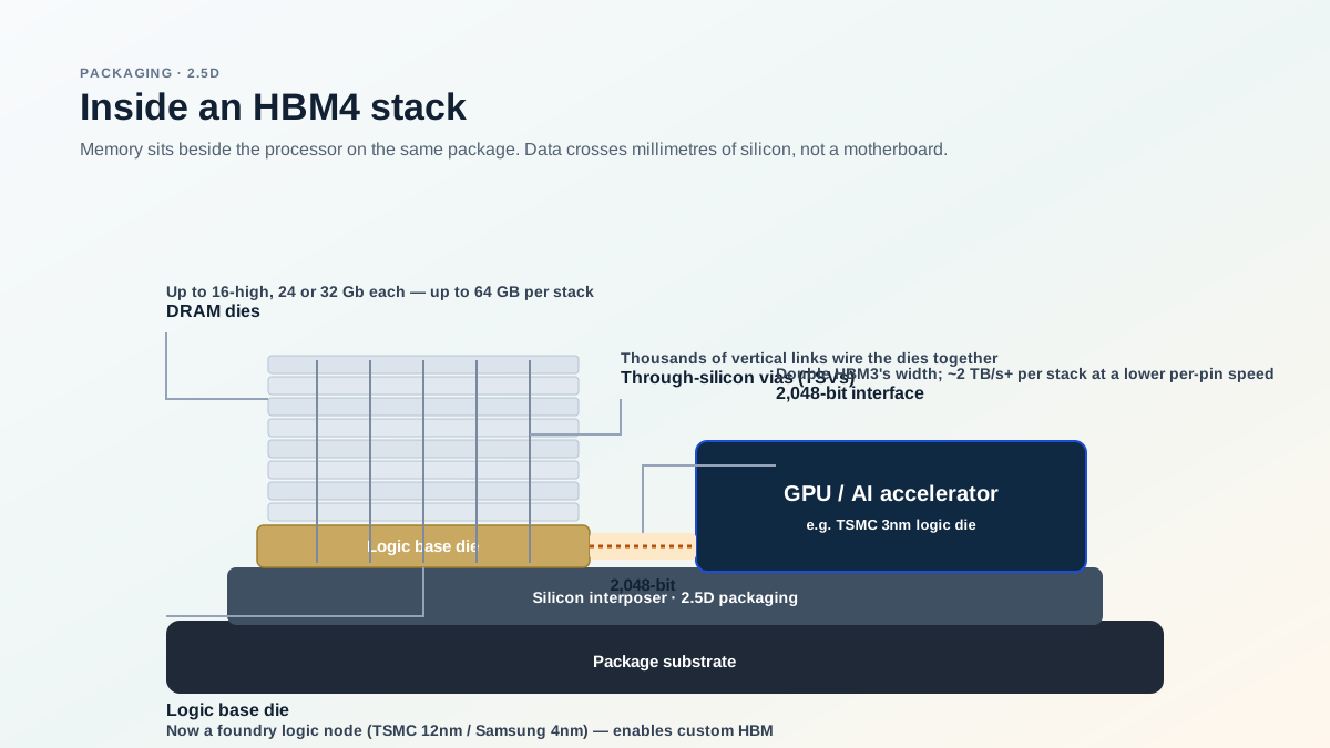
The 2,048-bit interface
The headline change is width. Against HBM3's 1,024-bit bus, HBM4's 2,048-bit interface doubles the number of data lines per stack. JEDEC sets the baseline per-pin speed at 8 gigabits per second, which yields about 2 terabytes per second of bandwidth per stack. The standard also doubles the number of independent channels, from 16 to 32, with two pseudo-channels each, adds Directed Refresh Management for stronger row-hammer protection, and keeps the interface backward-compatible with existing HBM3 memory controllers.
Commercial parts run well past the JEDEC floor. SK hynix and Samsung have tuned their HBM4 to roughly 10 to 11 gigatransfers per second, lifting per-stack bandwidth toward 2.5 to 2.8 terabytes per second. Nvidia runs the HBM4 in its Rubin GPU at about 10.8 gigatransfers per second, which is how eight stacks reach a combined 22 terabytes per second. The standard defines the floor; the buyers negotiate the ceiling.
Stacking and capacity
HBM4 supports 4-high, 8-high, 12-high and 16-high configurations, built from 24-gigabit or 32-gigabit dies, for a maximum of 64 GB in a single stack. The 12-high, 36 GB stack is the workhorse of the 2026 accelerators. At CES 2026, SK hynix showed a 16-high stack holding 48 GB. Height is not free: taller stacks trap heat, and keeping sixteen thinned dies flat enough to bond reliably is one of the hardest problems in the supply chain.
The base die moves to a foundry
The shift from a memory-process base die to a logic-process one is what makes HBM4 a platform rather than a faster part. Once the base die is fabricated on an advanced logic node, a supplier can build customer-specific features into it: tailored I/O, power management, or light data pre-processing sitting beneath the DRAM. The industry calls the result custom HBM, or cHBM.
SK hynix builds its HBM4 base die on TSMC's 12-nanometre logic process and has signalled it may move to TSMC's 3-nanometre node for the follow-on HBM4E. Samsung keeps the work in-house, pairing its sixth-generation 1c DRAM with a 4-nanometre foundry base die, a design it says clears 11 gigabits per second. TSMC and its design partner GUC have detailed a roadmap toward 3-nanometre (N3P) base dies for a custom C-HBM4E, targeting 12.8 gigatransfers per second, roughly double the power efficiency and about a 2.5-times performance uplift, with volume expected in 2027.
Power and efficiency
HBM4 lets suppliers pick lower operating voltages, with vendor-specific VDDQ options of 0.7, 0.75, 0.8 or 0.9 volts, and it trims energy per bit against HBM3. That matters because memory is a large and growing share of an accelerator's power draw, and the electricity budget of an AI cluster is now a line item that data-centre operators in Singapore and elsewhere plan around as carefully as floor space.
HBM4 benefits and enterprise use cases
HBM4's value is bandwidth per watt: it lets one accelerator hold a larger model and feed its compute units fast enough to keep them busy, which is the line between a GPU that serves tokens at a profit and one that stalls waiting for data.
In training, memory bandwidth sets how quickly parameters and activations move between compute and storage, and capacity sets how much of a model fits on each device before it has to be split across many. A Rubin GPU's 288 GB lets a large model sit on fewer devices, which cuts the traffic that would otherwise cross slower interconnects. Fewer shards, less coordination overhead, higher utilisation.
In inference, the constraint is usually the key-value cache — the running memory of a conversation that grows with context length and batch size. Long context windows and high concurrent user counts are memory problems first and compute problems second. HBM4's width is aimed squarely at that bottleneck, which is why the hyperscalers designing their own AI accelerators — Google's TPU line, Amazon's Trainium, and the Broadcom-built ASICs behind several large model providers — are pulling HBM4 alongside Nvidia and AMD.
High-performance computing keeps its long-standing claim on the technology, from weather modelling to molecular simulation, where memory bandwidth has always governed real throughput more than the peak floating-point numbers on a spec sheet.
For enterprises in Singapore and the wider region, the relevance is indirect but real. The AI clusters going into local and regional data centres run on these parts, and a buyer specifying GPU servers in 2026 is, whether they track it or not, buying a position in the HBM4 supply chain.
The regional constraint is as much power as silicon. Singapore lifted a multi-year pause on new data centres and, through the Infocomm Media Development Authority's Green Data Centre Roadmap of 30 May 2024, set out at least 300 megawatts of additional capacity in the near term, with a further potential 200 megawatts tied to green-energy deployment, alongside a target power-usage-effectiveness at or below 1.3 at full IT load. HBM4's efficiency gains speak directly to that limit: in a market where megawatts are rationed, memory that delivers more bandwidth per watt lets an operator field more compute inside a fixed power envelope. The component and the grid have become the same procurement problem.
HBM4 challenges, risks and limitations
HBM4's constraints are both physical and commercial: it is hard to package, expensive per gigabyte, thermally demanding, and, for 2026, effectively sold out.
The tightest chokepoint is not the DRAM but the packaging. Placing HBM stacks next to a large GPU on an interposer requires advanced 2.5D packaging capacity, most of it TSMC's CoWoS lines, and that capacity has trailed demand through the entire AI cycle. Hybrid bonding, through-silicon-via yield and the warpage of 16-high stacks all cap how fast supply can grow, regardless of how many DRAM wafers a maker can start.
Cost is the next barrier. Market trackers put HBM4 at roughly US$550 for a 12-high 36 GB stack, against about US$300 for an HBM3E stack of the same height. An accelerator carrying eight stacks therefore holds several thousand dollars of memory before the logic die, the interposer or the assembly is counted. Memory has become one of the largest bill-of-materials lines in an AI server.
Supply is the barrier buyers feel first. Industry trackers describe HBM as sold out for 2026, its output committed to Nvidia, AMD and a short list of custom-silicon customers before the year began. Because a wafer converted to HBM produces on the order of three times less usable capacity than one making standard DDR5, every stack the makers build subtracts from the pool of conventional DRAM. That trade-off, not a factory fire or a demand spike in PCs, is the mechanism behind the 2026 price surge covered below.
Concentration is the structural risk. Three companies make HBM, one of them supplies most of it, and nearly all of it is produced in Korea, with assembly increasingly routed through a small number of advanced-packaging sites. Micron's US$7 billion HBM packaging plant in Singapore is one of the first meaningful additions to that geography. Custom base dies raise a second kind of lock-in: a memory stack tuned to one accelerator is not a drop-in replacement, and qualification cycles run to many months, which narrows a buyer's room to switch suppliers when supply tightens.
Policy is now part of the supply map. On 2 December 2024, the United States Bureau of Industry and Security added high-bandwidth memory to the Commerce Control List under export classification 3A090.c, restricting the sale of advanced HBM — stacks with a memory-bandwidth density above 2 gigabytes per second per square millimetre — to China, and extending the rule to foreign-made parts built with US technology. The measure removed a large block of potential demand from the open market and reinforced the concentration of advanced HBM among a handful of US-aligned suppliers. For buyers outside China, the near-term effect is more supply pointed their way; the longer-term effect is a memory market whose allocation now follows trade policy as well as price.
The three-supplier race and the 2026 memory squeeze
The HBM4 market is a three-horse race feeding two dominant buyers, and in 2026 demand runs so far ahead of supply that memory, not logic, has become the semiconductor industry's pricing story.
Who makes HBM4
SK hynix set the pace. It declared the world's first HBM4 ready for mass production in September 2025 — doubling bandwidth and lifting power efficiency about 40 per cent over the prior generation — holds the largest single share of the HBM market, in the mid-to-high 50s per cent in 2026 (down from roughly 70 per cent a year earlier as rivals ramp), and has reportedly secured close to 70 per cent of Nvidia's initial HBM4 orders. Its base die is built on TSMC's 12-nanometre process, and it is targeting mass production of the 16-high, 48 GB part around the third quarter of 2026.
Samsung is the comeback story. After lagging on HBM3E, it built HBM4 on its 1c DRAM and an in-house 4-nanometre base die, cleared Nvidia's validation, and by August 2026 was reported to have lifted HBM4 yields to around 80 per cent, up from below 60 per cent when mass production began in February. It began shipping HBM4 to Nvidia and AMD early in 2026 and used Nvidia's March GTC event to unveil the faster HBM4E.
Micron is the third force and the one with the clearest Singapore footprint. The company is in high-volume production of HBM4 designed for Nvidia's Vera Rubin platform, and analysts have it closing on, or overtaking, Samsung for the number-two position in HBM. Its US$7 billion advanced-packaging facility in Singapore, which begins operations in 2026, is where a growing share of that HBM will be assembled.
Who buys it
Two customers set the tempo. Nvidia's Rubin, in volume in the second half of 2026, pairs 288 GB of HBM4 and 22 terabytes per second of bandwidth with a TSMC 3-nanometre GPU; at the rack level, an NVL72 system holds 20.7 terabytes of HBM4 and moves 1.6 petabytes per second of memory bandwidth. AMD's answer, the Instinct MI450 and MI455X, carries 432 GB of HBM4 and up to 23.3 terabytes per second per GPU, with its Helios rack holding 31 terabytes of the memory.
Behind the two GPU vendors sit the hyperscalers' own accelerators, and they are no longer a rounding error. Google's TPU, Amazon's Trainium and Trainium2, and the Broadcom-built chips behind several large model providers each consume HBM in volume, and the memory makers now treat custom base dies as a way to win that business directly. The logic base die that defines HBM4 is, in commercial terms, a door into the ASIC market: a supplier that can tailor the bottom of the stack to a customer's chip is selling engineering, not just a component. That is why the three makers are guiding record capital spending into HBM and advanced packaging even as they warn that returns depend on a build-out no one can guarantee past 2027.
The 2026 memory squeeze
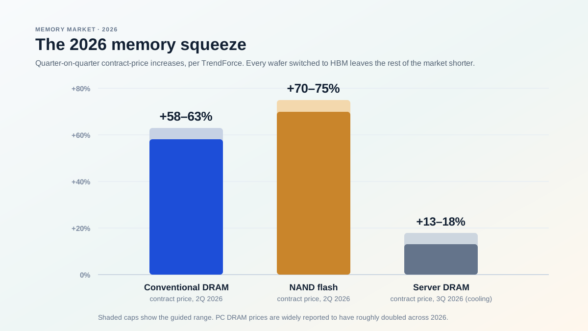
The diversion of capacity to HBM collided with an AI-driven surge in ordinary server memory, and the two together produced the sharpest memory inflation the industry has recorded. TrendForce reported that first-quarter 2026 DRAM industry revenue jumped about 81 per cent quarter on quarter as contract prices surged. It guided second-quarter conventional DRAM contract prices up 58 to 63 per cent and NAND flash up 70 to 75 per cent quarter on quarter, before weaker consumer demand moderated third-quarter server-DRAM increases to 13 to 18 per cent.
The pressure did not stay in DRAM. NAND flash and enterprise SSDs climbed alongside it as hyperscalers swapped nearline hard drives for flash to feed AI inference, and PC DRAM is widely reported to have roughly doubled across 2026. A procurement team refreshing a database cluster or a storage array is paying for a shortage created by a component it will never install.
The demand behind the squeeze is large and, for now, uninterrupted. Micron has told investors it expects the total HBM market to grow from roughly US$35 billion in 2025 to about US$100 billion in 2028, a compound rate near 40 per cent. TrendForce projects HBM4 becoming the mainstream product in the second half of 2026, with demand rising sharply year on year. Most forecasters expect supply to stay tight through 2026, with a possible turn late in 2027 and broader relief not before 2028.
The effect compounds down the purchase order. A mid-sized enterprise in Singapore refreshing a virtualisation cluster in 2026 faces much the same DRAM pricing as a hyperscaler, because both draw from one constrained pool, and a storage upgrade competes for NAND with the enterprise SSDs that AI inference has made scarce. Lead times on high-capacity modules stretch from weeks to months, and quotes that once held for a quarter now lapse in weeks. Finance teams that modelled a routine three-year hardware cycle on flat or falling memory prices are rewriting those assumptions mid-year.
HBM4 vs HBM3E, and HBM vs conventional DRAM
Against HBM3E, HBM4 is a step change in width rather than clock speed; against conventional DRAM, it is a different tool for a different job, not a faster version of the same one.
| Specification | HBM3E | HBM4 |
|---|---|---|
| Interface width per stack | 1,024-bit | 2,048-bit |
| Independent channels | 16 | 32 (2 pseudo-channels each) |
| Baseline pin speed (JEDEC) | up to ~9.6 Gb/s | 8 Gb/s baseline (parts tuned to 10-11 GT/s) |
| Bandwidth per stack | ~1.2 TB/s | ~2 TB/s baseline; ~2.5-2.8 TB/s in shipping parts |
| Max stack height | 12-high | 16-high |
| Max capacity per stack | 36 GB | 64 GB (32 Gb die, 16-high) |
| Base (logic) die | memory process | foundry logic node (e.g. TSMC 12nm, Samsung 4nm) |
| First volume year | 2024 | 2026 |
The move from HBM3E to HBM4 is defined by the doubled interface. HBM3E reached its bandwidth by pushing per-pin speed on a 1,024-bit bus; HBM4 widens the bus to 2,048 bits and lets the makers run each pin more conservatively, which helps both bandwidth and energy per bit. Capacity rises with the taller 16-high option, and the logic base die adds the customisation that HBM3E could not offer. Because HBM4 stays compatible with HBM3-class controllers, system designers can adopt it without redrawing the memory subsystem from scratch.
HBM against standard DRAM is a starker contrast. A DDR5 module or the newer MRDIMM is built for capacity and cost per bit, feeding CPUs that need large, affordable pools of memory. LPDDR trades bandwidth for low power in laptops and phones. HBM is built for bandwidth beside an accelerator, and it is far too expensive and too hard to package to serve as general-purpose memory. These are complements, not substitutes, which is precisely why diverting fab capacity from one to the other creates a shortage rather than a simple reshuffle.
The last distinction is commercial: merchant HBM versus custom HBM. A merchant part is a standardised stack any qualified buyer can order. A custom stack, enabled by the new logic base die, is tuned to one customer's accelerator. Custom HBM can lift performance and efficiency, but it deepens the tie between buyer and supplier and lengthens the qualification cycle, which is a governance question for any organisation that values a second source.
| Supplier | HBM position | HBM4 approach | 2026 status |
|---|---|---|---|
| SK hynix | Market leader (~mid-to-high 50s % share) | TSMC 12nm base die; first to mass-production readiness | ~70% of Nvidia HBM4 orders; 16-high 48GB targeted ~Q3 |
| Samsung | Recovering #2 / #3 | 1c DRAM + in-house 4nm base die; >11 Gb/s | Yields ~80% by August; shipping to Nvidia and AMD; HBM4E shown at GTC |
| Micron | Rising #2 / #3 | High-volume HBM4 for Vera Rubin; US$7B Singapore packaging | Volume production; Singapore line begins operating in 2026 |
Shares and order figures are as reported by TrendForce and the trade press; treat single-point share numbers as estimates in a market that is moving quarter to quarter.
Future outlook: HBM4E and supply relief
The HBM roadmap already runs past HBM4: a faster HBM4E in 2027, logic base dies on 3-nanometre nodes, and a market Micron expects to roughly triple by 2028.
HBM4E is the next step, and it is where the base-die shift pays off. TSMC and GUC have laid out custom C-HBM4E designs built on 3-nanometre (N3P) base dies, aiming at 12.8 gigatransfers per second with roughly double the power efficiency and about a 2.5-times performance uplift, and volume expected in 2027. SK hynix is reportedly weighing TSMC's 3-nanometre node for its own HBM4E logic dies to keep pace with Samsung's in-house approach. The competitive front is moving from the DRAM itself to the logic underneath it.
Capacity is the other race. Micron's Singapore packaging plant, which begins operating in 2026 and expands from 2027, adds a new node of advanced-packaging capacity outside Korea and Taiwan and slots into a Singapore ecosystem that already accounts for around a tenth of world chip output and close to a fifth of global semiconductor-equipment production. New DRAM fabs and packaging lines in Korea and the United States will add supply through the decade. Whether that catches demand is the question every forecaster hedges: most see tightness easing late in 2027 at the earliest, with real relief closer to 2028.
Further out, the makers are sketching high-bandwidth flash as a cheaper capacity tier beneath HBM, and the standards bodies have begun the early work on the generation after HBM4E. None of that changes the near-term picture. HBM4 is the memory of the 2026-2027 AI build-out, and its supply is spoken for.
Frequently asked questions
What is the difference between HBM4 and HBM3E?
HBM4 doubles the memory interface from 1,024 bits to 2,048 bits per stack, raising baseline bandwidth to about 2 terabytes per second, and supports taller 16-high stacks of up to 64 GB. It also moves the base die to a foundry logic process, which HBM3E did not do. HBM3E remains a 1,024-bit part that reached its bandwidth through higher pin speed.
When is HBM4 available?
JEDEC published the HBM4 standard in April 2025. SK hynix declared mass-production readiness in September 2025, Samsung began shipping to Nvidia and AMD in early 2026, and Micron reached high-volume production for Nvidia's Vera Rubin platform. HBM4 becomes the mainstream HBM product in the second half of 2026.
Why is HBM4 so expensive?
It is hard to build and hard to package. Advanced 2.5D packaging capacity, mainly TSMC's CoWoS, is the binding constraint, and 16-high stacking pushes yield limits. Market trackers estimate roughly US$550 for a 12-high HBM4 stack against about US$300 for HBM3E, and each accelerator uses eight stacks.
Is HBM4 behind the 2026 memory shortage?
Indirectly, yes. Producing HBM consumes advanced wafer capacity at roughly three times the rate of standard DDR5, so makers shifting output to HBM shrink the supply of conventional DRAM. Combined with AI-driven demand for server memory, that drove record contract-price increases across DRAM, NAND and enterprise SSDs in 2026.
Who makes HBM4, and who supplies Nvidia first?
Three companies make it: SK hynix, Samsung and Micron. SK hynix leads on share and reportedly holds most of Nvidia's initial HBM4 orders, while Samsung cleared Nvidia's validation and began shipping in early 2026. All three are qualified into Nvidia's Rubin generation.
What is custom HBM (cHBM)?
Custom HBM uses the HBM4 logic base die — now built on a foundry process such as TSMC 12nm — to add customer-specific features like tailored I/O or power management beneath the DRAM. It can improve performance for one accelerator but deepens the buyer's dependence on a single supplier.
SEO Recommendations
Suggested internal links
- Computer Memory Hierarchy Explained — Link from the opening definition so readers can place HBM against cache, DRAM and NAND.
- How GPUs Work for AI — Link from the benefits section, where HBM feeds the GPU compute units.
- NVIDIA Technologies Explained — Link from the buyers section for the rack-scale Rubin and NVLink context.
- AI Data Centre Infrastructure — Link from the Singapore power discussion to the data-centre capacity picture.
- Singapore's Semiconductor Value Chain — Link from the future-outlook section on Singapore's packaging ecosystem.
Image placement suggestions
- Inside the technical breakdown — alt text: Cutaway of an HBM4 stack showing DRAM dies, through-silicon vias, and a foundry-built logic base die on a silicon interposer beside a GPU.
- In the memory-squeeze section — alt text: Bar chart of 2026 memory contract-price increases: conventional DRAM +58-63% and NAND +70-75% in 2Q26, moderating to +13-18% for server DRAM in 3Q26.
Additional long-tail keyword opportunities
- HBM4 vs HBM3E specifications
- HBM supply chain 2026 shortage
- why are DDR5 and SSD prices rising 2026
- HBM4 procurement enterprise buyers
- custom HBM cHBM logic base die
- Micron Singapore HBM packaging facility
- Nvidia Rubin 288GB HBM4 bandwidth
Sources and further reading
- JEDEC — JESD270-4 HBM4 Standard press release (16 April 2025)
- TechPowerUp — JEDEC and industry leaders release the JESD270-4 HBM4 standard
- SK hynix Newsroom — Completes world's first HBM4 development and readies mass production (Sept 2025)
- TrendForce — Samsung's HBM4 yield reportedly hits 80% as the Vera Rubin race heats up (10 Aug 2026)
- Singapore EDB — Micron breaks ground on US$7B HBM advanced-packaging facility in Singapore
- NVIDIA — Vera Rubin NVL72
- AMD — Instinct MI400 Series GPUs (432 GB HBM4)
- TechPowerUp — AMD previews 432 GB HBM4 Instinct MI400 GPUs and the Helios rack
- TrendForce — Rapid contract-price surge drives 1Q26 DRAM industry up 81% QoQ
- TrendForce — AI server demand to drive memory contract-price increases in 2Q26
- Tom's Hardware — TSMC and GUC detail HBM4, HBM4E and C-HBM4E: 3nm base dies, up to 12.8 GT/s by 2027
- U.S. BIS / Commerce — Foreign-Produced Direct Product Rule additions adding HBM under ECCN 3A090.c (2 Dec 2024)
- IMDA — Singapore announces Green Data Centre Roadmap (30 May 2024)
- Singapore EDB — What makes Singapore a prime location for semiconductor companies
- Computer Memory Hierarchy Explained: Cache, DRAM, NAND, HBM and Storage
- How GPUs Work for AI: From CUDA Cores to AI Factories
- NVIDIA Technologies Explained: CUDA, GPUs and the AI Infrastructure Stack
- AI Data Centre Infrastructure: Power, Cooling and GPU Cluster Demand
- How a Chip Gets Made: Singapore's Semiconductor Value Chain Explained